Contents
Overview
This product has an SX1301/SX1308 baseband processor and two SX1257/SX1255 RF frontend chips, and peripheral circuits onboard. and it could listen on multiple channels and decode packets sent with different LoRa spreading factors simultaneously. This concentrator module is supposed to connect to a host controller via SPI interface. A host controller could either be an MCU with an SPI interface or a PC with a USB to SPI converter located between the concentrator and PC. All the RF jobs are done within this concentrator module and the user could focus on high-level software development. HAL source files are provided by Semtech who is the manufacturer of the baseband processor.
Features
- 4V-12V wide range supply voltage
- +-1ppm TCXO
- Compact size 70mm x 34mm
- 50ohm RF port
- ESD protected digital IO
- Plug and play design for Raspberry Pi
Pin Configuration
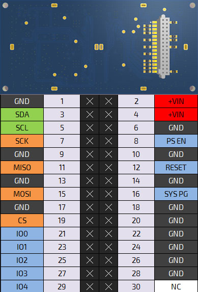
| Pin No. | Pin Name | Pin Type | Description |
| 1 | GND | Power | Power ground. |
| 2 | +VIN | Power | Power supply. |
| 3 | SDA | Open Drain | SDA of the onboard 24AA02E64T EEPROM chip. Could be left unconnected if not used. |
| 4 | +VIN | Power | Power supply. |
| 5 | SCL | Open Drain | SCL of the onboard 24AA02E64T EEPROM chip. Could be left unconnected if not used. |
| 6 | GND | Power | Power ground. |
| 7 | SCK | Input | SCK of the SPI interface. |
| 8 | PSEN | Input | Power supply enable pin, active HIGH, internally pulled-up. A LOW voltage on this pin disable the power converters onboard. Could be left unconnected if not used. |
| 9 | GND | Power | Power ground. |
| 10 | GND | Power | Power ground. |
| 11 | MISO | Output | MISO of the SPI interface. |
| 12 | RESET | Input | Baseband processor reset pin. Active HIGH. |
| 13 | GND | Power | Power ground. |
| 14 | GND | Power | Power ground. |
| 15 | MOSI | Input | MOSI of the SPI interface. |
| 16 | SYSPG | Open Drain | System power good pin. This pin is internally pulled-up. A HIGH level indicates that the onboard power converters are working well, while a LOW level indicates that there is something wrong with the onboard power converters. This pin could be left unconnected if not used. |
| 17 | GND | Power | Power ground. |
| 18 | GND | Power | Power ground. |
| 19 | #CS | Input | #CS pin of the SPI interface. Active LOW. |
| 20 | GND | Power | Power ground. |
| 21 | IO0 | IO | GPIO0 of the baseband processor. |
| 22 | GND | Power | Power ground. |
| 23 | IO1 | IO | GPIO1 of the baseband processor. |
| 24 | GND | Power | Power ground. |
| 25 | IO2 | IO | GPIO2 of the baseband processor. |
| 26 | GND | Power | Power ground. |
| 27 | IO3 | IO | GPIO3 of the baseband processor. |
| 28 | GND | Power | Power ground. |
| 29 | IO4 | IO | GPIO4 of the baseband processor. |
| 30 | NC | NC | Not used. |
u.fl Connector 1: Pulse Per Second input to connect to external GPS
u.fl Connector 2: RF signal port
Absolute Maximum Ratings
| Parameter | Min. | Max. | Unit |
| Supply Voltage(+VIN) | -0.3 | 12.5 | V |
| IO Pin Voltage | -0.3 | 3.6 | V |
| Operating Temperature | – | 75 | Celsius |
Electrical Characteristics
T=25C, +VIN=5V, unless otherwise specified
| Parameter | Condition | Min. | Typ. | Max. | Unit |
| Operating Supply Voltage | – | 4.0 | 5.0 | 12V | V |
| Current Consumption | All channels active, radio A ON, radio B ON, receiving mode | – | 370 | 420 | mA |
| Current Consumption | Continous wave transmitting at 20dBm | – | 195 | 210 | mA |
| Logic low input threshold | – | 0.4 | – | – | V |
| Logic high input threshold | – | – | – | 2.9 | V |
| Logic low output level | – | 0 | – | 0.4 | V |
| Logic high output level | – | 3.9 | – | 3.3 | V |
RF Performance Data
Continuous Wave Transmitting Power Test
| Dig | Mix | PA | Tx Power |
| 3 | 8 | 0 | -10dBm |
| 3 | 15 | 0 | 1dBm |
| 0 | 8 | 0 | -4dBm |
| 0 | 15 | 0 | 3dBm |
| 0 | 8 | 1 | 6dBm |
| 0 | 15 | 1 | 14dBm |
| 0 | 8 | 3 | 21dBm |
| 0 | 15 | 3 | 26dBm |
dig=3, mix=8, pa=0

dig=3, mix=15, pa=0

dig=0, mix=8, pa=0

dig=0, mix=15, pa=0

dig=0, mix=8, pa=1

dig=0, mix=15, pa=1

dig=0, mix=8, pa=3

dig=0, mix=15, pa=3

LoRa Packet Transmitting Test
dig=0, mix=15, pa=1, LoRa Modulation, SF=7, BW=125KHz

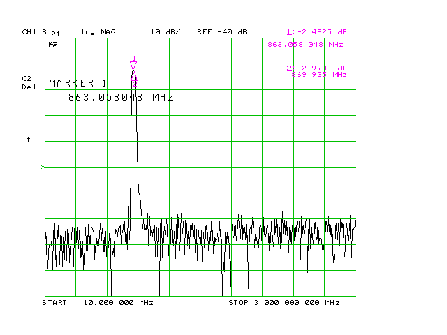
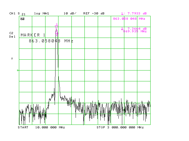
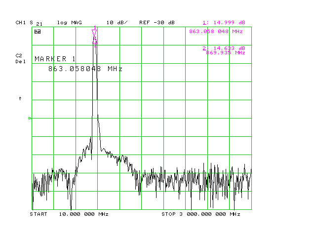
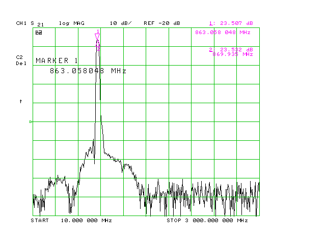
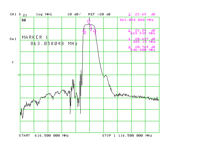
Tx Path Gain Measure Result
Port1: Pin2 of U17, -10dBm input
Port2: Center pin of the u.fl connector
PA Gain: GAIN8=0, GAIN 16=0
PA Gain: GAIN8=1, GAIN 16=0
PA Gain: GAIN8=0, GAIN 16=1
PA Gain: GAIN8=1, GAIN 16=1
PA Gain: GAIN8=1, GAIN 16=1 with 866.5MHz CF and 500MHz Span
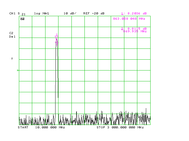
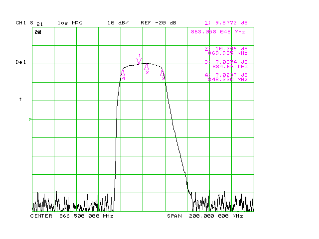
Rx Path Gain Measure Result
Port1: Center pin of the u.fl connector
Port2: Pin27 of U19
866.5MHz CF and 500MHz Span
Typical Application with Raspberry Pi
We have created a step-by-step installation guide for Raspberry Pi users. Please click here.
Resources
- HAL Library
- Raspberry Pi Application Guide
Assembly Drawings
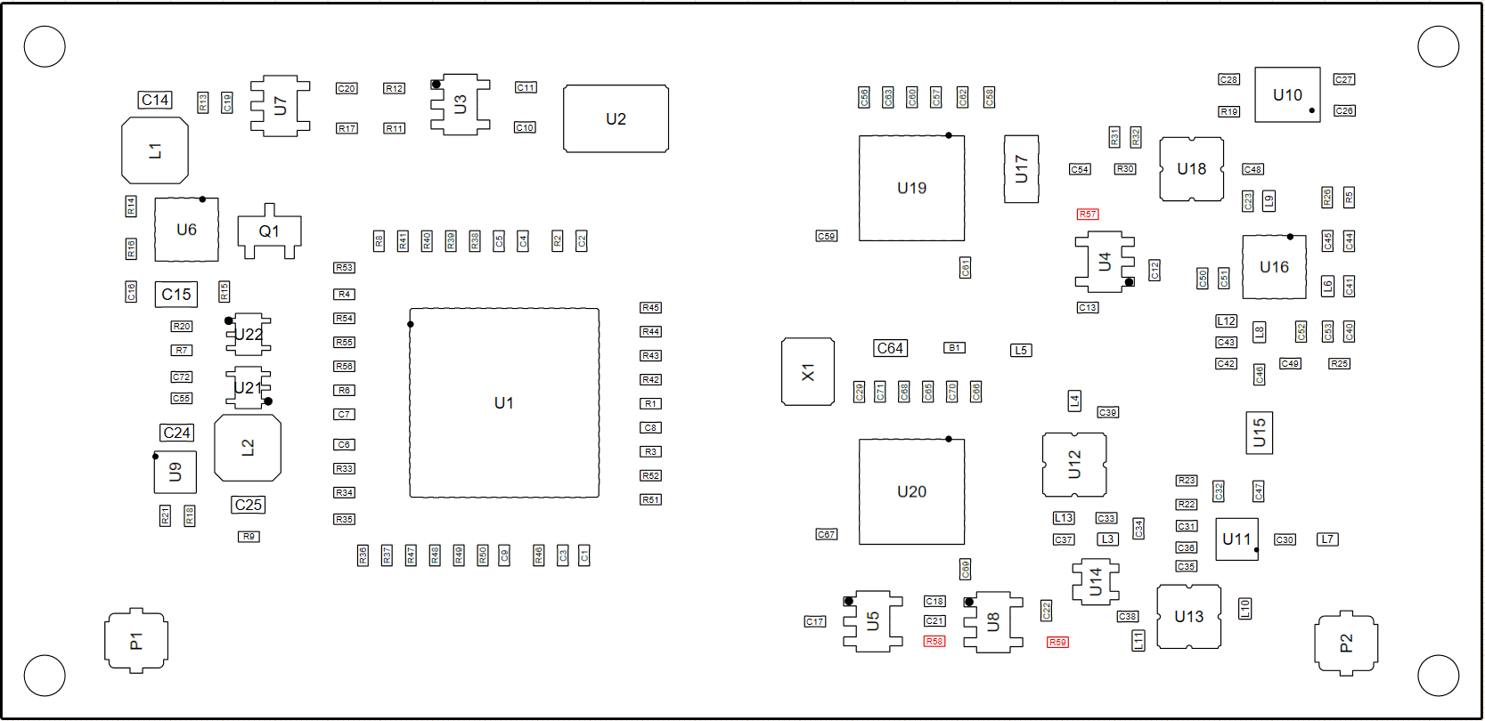
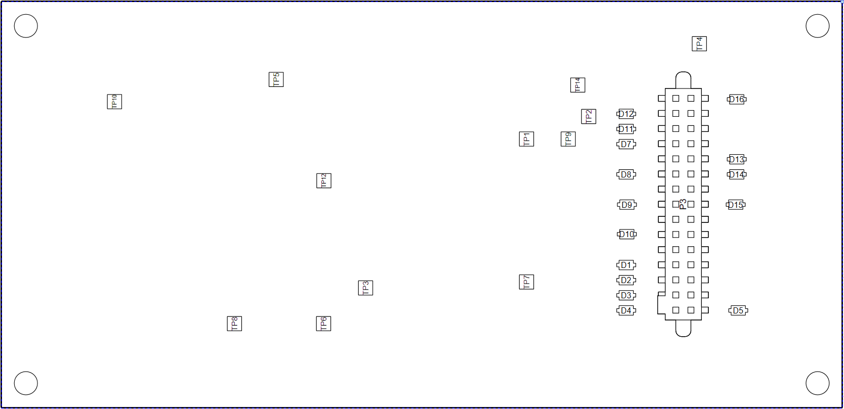
Right-click the above images and choose “save image as” to view a full-size picture.
Dimensions

Schematics are available after purchase, please contact us via Email.