Contents
Overview
This module is designed to enable long range I2C communications which extends the cable length from several meters to 300 meters. It is ideal for applications that need to run over long wires such as the CAT5e Ethernet cable that is commonly used to make connections between rooms. The signals are transmitted via balanced transmission lines (twisted pairs) which greatly reduces noise and extends the range. NXP PCA9600 I2C bus extender IC is used as the main component on this module. The PCA9600 is designed to isolate I²C-bus capacitance, allowing long buses to be driven in point-to-point or multipoint applications. It can operate at speeds up to at least 1 MHz.
Features
- Bidirectional data transfer of I2C-bus signals
- 100 kHz operation on 300 meters of wire
- 1 MHz operation on 20 meters of wire
- On-board boost converter
- 12V/24V (configurable) power output
Pin Configuration
- Device end:
- SCL: I2C SCL
- SDA: I2C SDA
- 5V0: Power input to the module
- GND: GND
- VPU: (optional) SCL/SDA pull-up voltage input (connected to 5V0 by default. It can be disconnected from 5V0 bus when pull-up voltage other than 5V is needed.)
- VBUS: (optional) Power supply output of the on-board DC-DC converter.
- Wire end:
- SCL_L: Negative pin for the SCL differential transmission wire
- SCL_H: Positive pin for the SCL differential transmission wire
- SDA_L: Negative pin for the SDA differential transmission wire
- SDA_H: Positive pin for the SDA differential transmission wire
- GND: (optional) GND. As the communication is differential, there is no need to share a command ground across the wire, especially when the two systems across the wire are at different ground levels.
- VBUS: (optional) Power supply output of the on-board DC-DC converter
Possible Wiring Scheme
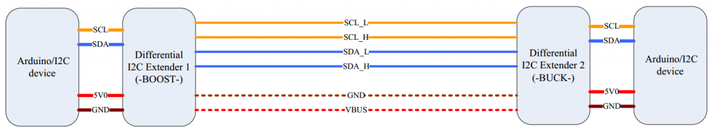
- Point-to-point operation
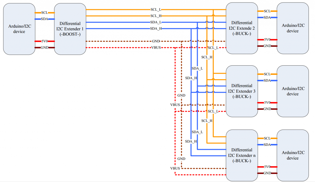
- Multidrop operation
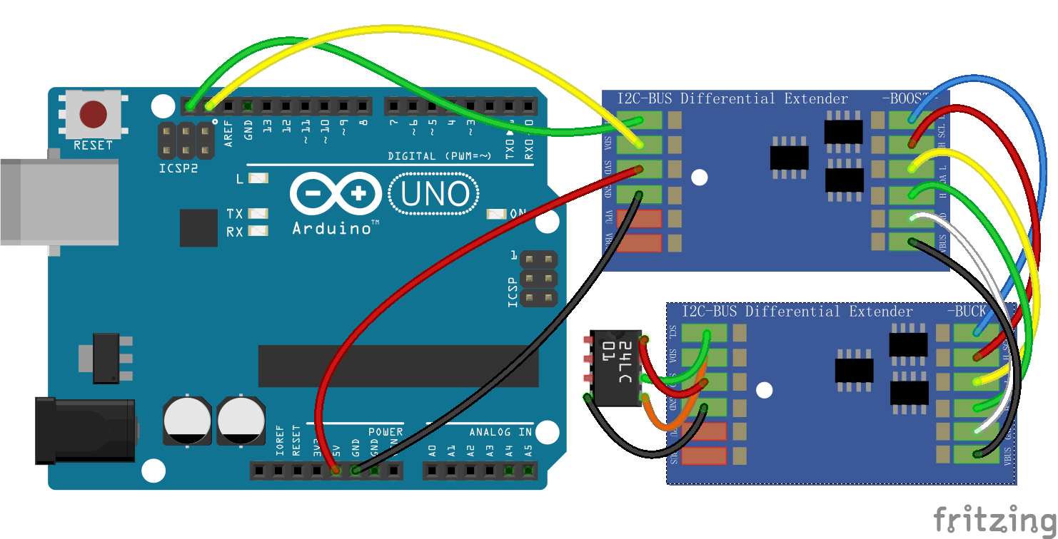
- Arduino Wiring Scheme
- Raspberry Pi Wiring Scheme
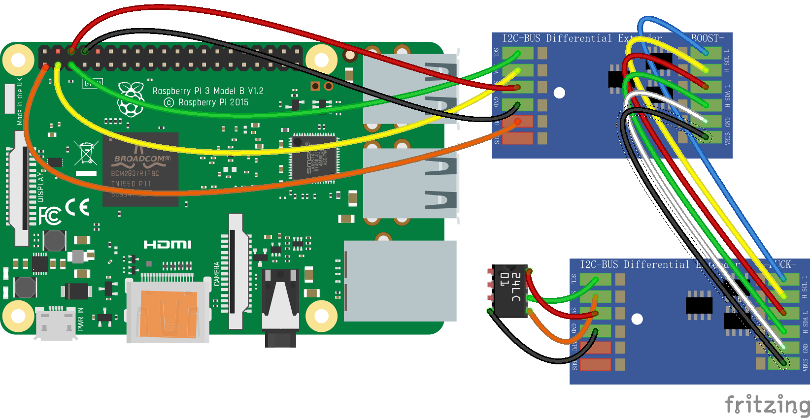
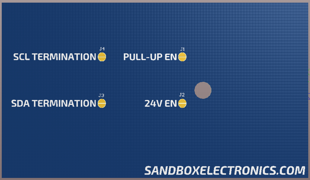
To use with Raspberry Pi, user should desolder the solder jumper named “PULL-UP EN” on the back of the module.
Technical Details
SCL and SDA of the I2C interface is bidirectional by its definition. The PCA9600 on the module is used in such a way that it splits SCL into two unidirectional signal, named SCL_TX, and SCL_RX. The same applies to SDA signal. The purpose to split these two signals is that the PCA82C251T differential transceiver requires unidirectional signals.
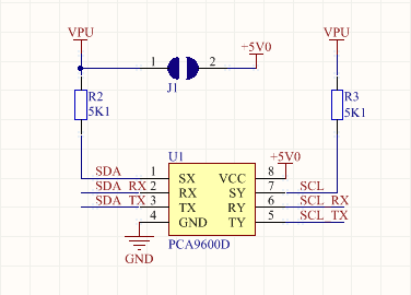
As shown in he picture above, the J1 could be used to power the VPU to 5V or to disconnect it from 5V. By factory default, VPU is connected to 5V0.
If SCL is driven by local I2C device to logic “0”, the SCL_TX will be logic “0”. Then the SCL_TX will be transmitted as a “dominant” symbol on the SCL_H and SCL_L by PCA82C251T transceiver. At the same time, The RXD pin of PCA82C251T driving the SCL_RX signal to logic “0”, because there is a “dominant” symbol on the SCL_H and SCL_L. PCA9600 keeps sensing the logic state of the SCL_RX, and keeps the SCL to logic “0”. In I2C definition a logic “0” is the dominant bit, so this configuration is consistent with the I2C specification.
If SCL is driven by local I2C device to logic “1”, the SCL_TX will be logic “1”. Then the SCL_TX will be transmitted as a “recessive” symbol on the SCL_H and SCL_L by PCA82C251T transceiver.
- If there is someone driving the SCL_L to SCL_H to “dominant” state. PCA82C251T will output a logic “0” on its RXD pin, which drives the SCL_RX to logic “0”; Then PCA9600 will drive the SCL to logic “0” to acknowledge there is a conflict or start of frame on the bus.
- If there is someone is driving the SCL_L to SCL_H to “recessive” state or there is no other one driving the bus. PCA82C251T will output a logic “1” on its RXD pin, which drives the SCL_RX to logic “1”; Then PCA9600 will drive the SCL to logic “1”, which is the intended logic state of the local I2C device.
The same principles applied to SDA.
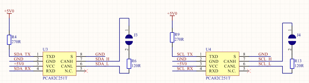
As shown in the picture above, there are two jumpers , one for each transceiver. The terminal resistor is required at each termination node on the bus. By factory default, both J3 and J4 are shorted, which means that the terminal resistors are connected to the bus by default.
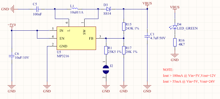
Another important feature of this module is that there is a on-board boost converter. As the module is designed for long range I2C communication and there are some scenarios user may want to supply power to the other side by wires. There are two optional output voltage available, 12V and 24V. Over long cables, to delivery the same amount of power, the higher the voltage, the less the copper loss. On the other hand, the higher the voltage, the lower the conversion efficiency of the boost converter. So it is up to the user to decide to use 12V or 24V on VBUS. For best overall power efficiency, the rule of thumb is to use 12V for short wires(less than 100m) and 24V for long wires.
The schematics of the boost converter is shown in the picture below. The output current capability of the boost converter is shown in the picture, too.
Here is some tests result made with and Arduino UNO and a HDC1050 humidity sensor.
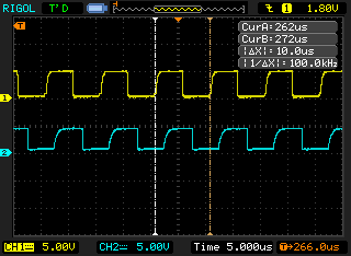
The picture below shows the waveform of SCL and SDA when the sensor is directly wired to Arduino via a 15cm length cable. CH1(yellow) is SCL and CH2(blue) is SDA.
Here comes the SCL waveform when connecting the sensor to Arduino via 300m length twisted pair cable.
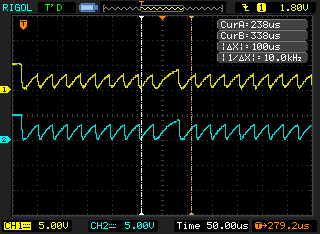
It could been seen from the picture above that the stray capacitance of the cable has seriously deformed the SCL waveform at both local(CH1) and remote(CH2) end.
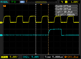
Here comes the SCL waveform shows the performance of our differential I2C extender with Arduino, HDC1050, and 300m twisted pair cable.
and if give it a closer look, we can actually see the propagation delay of the SCL signal.
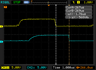
It could be read from the cursors in the picture the propagation delay of the SCL is about 1.76us. The propagation delay of the twisted pair cable is 4.8-5.3ns/m. Given the length of the cable which is 300m, the propagation delay should be 1.4- 1.6us. There are also some delay beween the differential transceivers and some measure erros. So The 1.76us reading is quite reasonable.
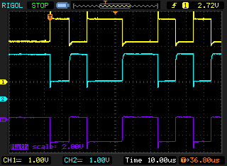
Here is the screenshot from the scope of the SCL_H and SCL_L signal.
- Blue – SCL_H
- Yellow – SCL_L
- Purple – SCL_H – SCL_L
Here are the locations of the jumpers on the back side of the PCB.
Resources
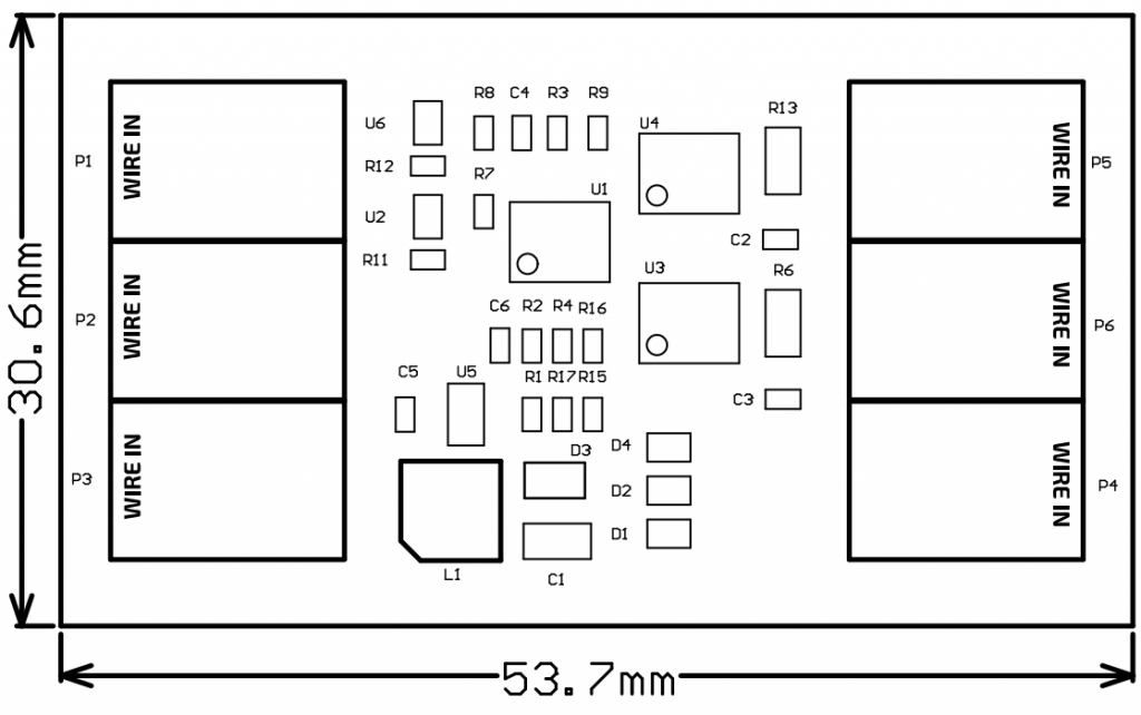
Dimensions
Full schematics is available, please contact us by email.